
Here’s the efficiency wire. The Korea Institute of Energy Research has put 26.7 per cent on a perovskite-on-CIGS tandem cell, and Germany’s Fraunhofer Institute for Solar Energy Systems has certified the number. The U.S. National Laboratory of the Rockies — NLR, the lab that used to answer to NREL — has parked the same result on its Best Research-Cell Efficiencies Chart. EurekAlert carried the National Research Council of Science and Technology release; Solar Now carried the same note around 4–5 September 2026. The prior mark was 26.3 per cent. Korea just moved it.
Call the stack by its right name. Perovskite on top. Copper indium gallium selenide — CIGS — on the bottom. Both layers are thin-film friendly, which is why the result is more than a lab vanity number. The certified cell is a sub-1 cm² research device. KIER’s own lab meter read 27 per cent before Fraunhofer ISE locked the official 26.7. That gap is normal. Certification is the story. The chart entry is the receipt.
You’re going to want the previous holder before you cheer. A joint Seoul National University and Korea Institute of Science and Technology team set 26.3 per cent in July 2025 for the same perovskite/CIGS, sub-1 cm² category. KIER’s Photovoltaic Research Department has now taken the crown inside Korea’s own pipeline. pv magazine Global dated the trade write-up 2 September. Newswise and the EurekAlert feed put the formal release at 4 September Eastern. I’m not inventing a third date. Certification house and chart first, then the wire that moved the press note into English.
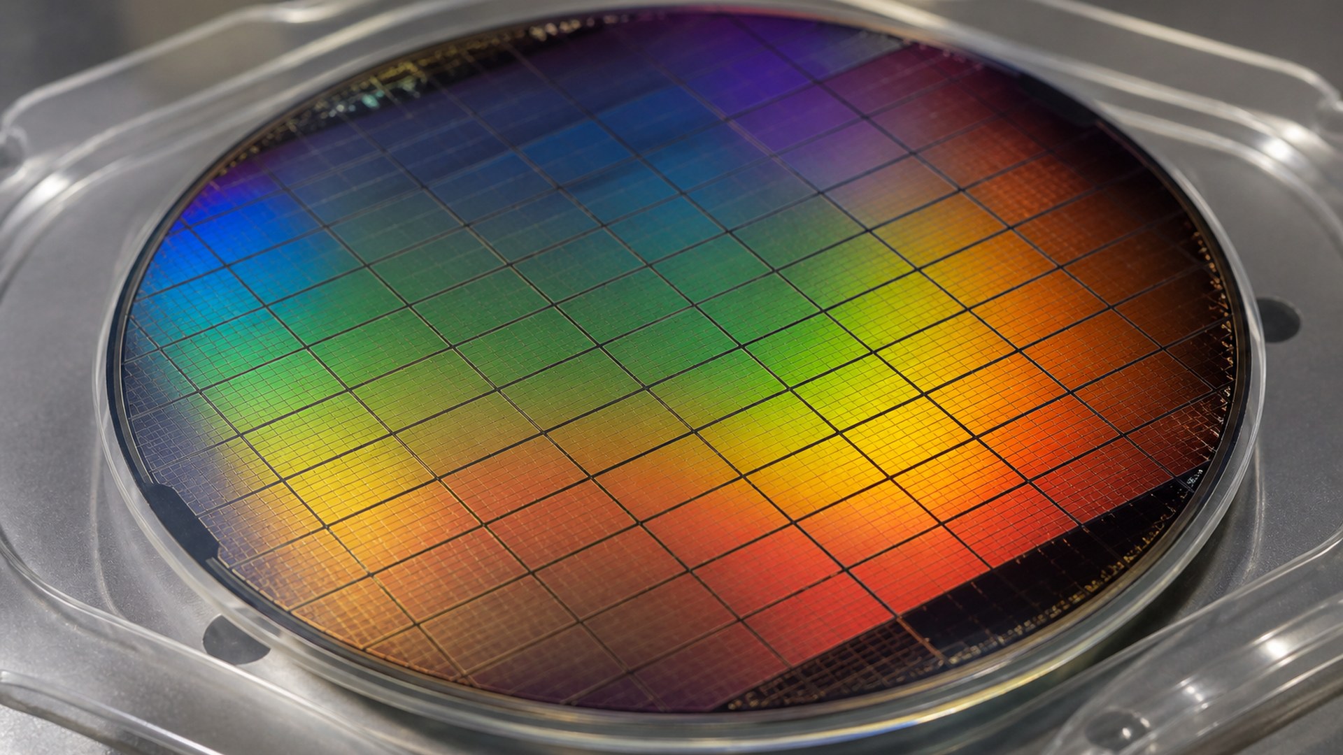
Why tandem, if silicon still owns the rooftops? Silicon is mature. The physical ceiling on a single-junction silicon cell is a known argument among people who live in bandgaps. Tandem stacks two absorbers with different spectral preferences so the top cell drinks the short wavelengths and the bottom cell keeps the longer ones. Perovskite is a strong top-cell candidate. CIGS is a thin-film bottom that can be fabricated without pretending you’re pouring a wafer fab. Put them together and you get a lightweight, potentially flexible laminate instead of a rigid crystalline slab. That is the product psychology KIER is selling alongside the percentage.
The hard part is the join. Integrating the two cells can damage the perovskite absorber. Some layers in the stack also eat light they were never meant to keep, which steals photocurrent from the meters. KIER says the team ran a root-cause pass on those losses, then built interfacial layer materials and process steps that spare the perovskite when the stack goes together. They also reworked the transparent top electrode and the charge-transport layers so parasitic absorption drops and the current the cell can deliver climbs. Senior researcher In-Young Jeong — also rendered Inyoung Jeong in the English releases — said the point of the week is that efficiency and stability can move together when you cut both interfacial and optical losses at once. That sentence is doing the science work for it.
Keep the area category straight. The 26.7 per cent record is for devices under 1 cm². For perovskite/CIGS tandems larger than 1 cm², the standing certified mark in the trade press is still 25.5 per cent, held by Germany’s Helmholtz-Zentrum Berlin with Humboldt-Universität and checked by the European Solar Test Installation. Different size bucket. Different chart line. Don’t mash them. Small-area research cells are where records land first; large-area modules are where money gets made. KIER is explicit that the next job is carrying the small-cell efficiency onto larger modules and talking to industrial partners about transfer. That is the honest next paragraph, not a hedge.
Applications language in the release is the part you can print without blushing. More watts per square metre is the terrestrial line — buildings and vehicles where area is scarce. The thin-film pitch then points at small satellites and, further out, space-based compute sites where mass and volume are the real currency. I’m not pretending a sub-centimetre research cell is flying tomorrow. Korea just posted a certified world record in a tandem architecture that is already being framed for light payloads. True where true. Speculative where labelled.
Metric, because we run metric. One square centimetre is the size class. Twenty-six point seven per cent is the certified conversion. Twenty-seven per cent is the in-house meter. Twenty-six point three was yesterday’s Korean record. Twenty-five point five is the large-area sibling you must not confuse with this one. Fraunhofer ISE is in Freiburg. NLR’s chart is the U.S. scoreboard the whole photovoltaics field still watches even after the lab’s rename. Those are the countable nouns.
What isn’t in the EurekAlert note is a commercial module efficiency, a factory name, or a ship date for flexible rooftops. What is in it: a second Korean institute in as many years has moved the perovskite/CIGS tandem line, an independent German certification lab put a stamp on it, and the U.S. best-cell chart now shows 26.7 where 26.3 used to sit. Energy reporting likes receipts. This one has three: Fraunhofer, NLR, and a prior Korean mark beaten in public.
Read the architecture once more if you’re reading for a general audience. Sunlight hits the perovskite first. The top cell converts the high-energy slice. What’s left drops into the CIGS bottom cell, which is tuned for a different bite of the spectrum. Because both absorbers can be deposited as thin films, the finished sandwich can, in principle, be light and bendable in ways a thick silicon wafer is not. Interface chemistry is why most tandems stall between a pretty lab slide and a durable product. KIER’s claim is that they found materials and process knobs that protect the perovskite during that marriage and cut optical waste in the top electrode stack. The certified percentage is how you know the knobs worked on this device.
Stability talk is cheap in photovoltaics press notes. Jeong’s line couples stability to the same loss-cutting work that raised the efficiency, which is a better sentence than a vague promise. Still treat durability as a research claim until outdoor and damp-heat datasets are the primary, not a quote. Scaling is the other honesty check. A champion cell under a square centimetre is how records are born. A module that keeps most of that efficiency across hundreds of square centimetres is how a country builds an industry. KIER says that handoff is now the programme. Collaborate with partners who care about mass production. Transfer the process. Push toward space-rated cells later. Roadmap, not inventory.
For the wire date, keep the sources straight. pv magazine’s Emiliano Bellini carried the trade story on 2 September with the Fraunhofer and chart language already in it. The National Research Council of Science and Technology package on Newswise and EurekAlert carries a 4 September Eastern timestamp. Solar Now republished the EurekAlert text around that window. Dong-A Science and the Herald Business carried Korean-language and English explainers in the same stretch. I’m citing the certification path and the Solar Now / EurekAlert lane, not inventing a press conference that wasn’t on the tape.
So on Sunday 6 September 2026: KIER, 26.7 per cent certified perovskite/CIGS tandem, Fraunhofer ISE stamp, NLR best-cell chart entry, prior 26.3 per cent from SNU/KIST beaten. Thin-film stack, perovskite top, CIGS bottom, sub-1 cm² research cell, 27 per cent on the lab meter. Interface and optical-loss work credited for the jump. Large-area scaling still ahead. EurekAlert and Solar Now carry the English lane. No invented module price. No invented factory. The fact on the wire is a certified world record in a tandem chemistry Korea has now moved twice. That is enough for a breaking energy lead: a number, a stamp, and a chart line you can point at.
The paper
Comments
No notes on this story yet.
Sign in to comment